Key Words: Silicon Wafer Dicing PCB Depaneling Glass Cutting
Home > News > Industry News
【Description】:
A comprehensive technical guide on PCB and FPCB laser circuit etching using UV picosecond lasers, covering process parameters, application scenarios, DFLE guidelines, and quality assurance.
Traditionally, circuit patterns on copper‑clad laminates (Cu/PI or Cu/LCP) are created by photochemical wet etching – a multi‑step process involving lamination, exposure, development, etching, and stripping. While well‑established, wet etching suffers from inherent limitations: undercut (side‑etch), chemical waste disposal, long cycle times, and difficulty in achieving ultra‑fine line/space below 50 µm.
Laser circuit etching (also referred to as PCB laser etching or copper laser ablation) offers a direct, mask‑less, dry alternative. A focused laser beam selectively removes unwanted copper from the substrate, leaving behind the desired conductive pattern. This technique is not only a game‑changer for FPC prototyping, but also enables fine line structuring, circuit repair, and even thin film metal patterning on various flexible and rigid substrates.
Among all laser sources, the UV picosecond laser (UV ps laser) has emerged as the optimal tool for this task, thanks to its “cold” ablation mechanism that minimises thermal damage to the underlying polyimide or liquid crystal polymer dielectric.
To appreciate the value of laser direct structuring, it is useful to compare it with the incumbent technology:
The UV picosecond laser combines the high absorption of copper at 355 nm with an ultra‑short pulse duration that removes material via photo‑mechanical and photo‑chemical mechanisms before heat can diffuse into the surrounding material. This is often described as “cold” ablation – the copper is vaporised or ejected as fine particles, while the underlying PI remains un‑yellowed and free from carbonisation.
For thin film circuit patterning – where metal layers may be only 5–12 µm thick – the UV ps laser provides the precision and selectivity needed to pattern without penetrating the dielectric.
Successful laser circuit etching requires careful optimisation of several inter‑dependent parameters. The goal is to completely remove copper in the scanned areas while leaving the substrate unscathed and achieving a clean, residue‑free trace edge.
The ablation threshold of copper for 355 nm, ps pulses is typically in the range of 0.3–0.6 J/cm².
For a spot size of ~20 µm (1/e²), this translates to pulse energies of 5–15 µJ.
Using a fluence just above threshold (1.2–1.5× threshold) ensures efficient removal with minimal heat spread. Excessive fluence causes copper melting and splatter, which re‑deposits as debris.
Unlike drilling a single hole, circuit etching involves raster‑scanning large areas. The beam traces parallel lines (hatch lines) with a certain overlap:
Hatch overlap (line‑to‑line spacing) should be 50–70% of the spot diameter.
Example: spot size = 20 µm → hatch spacing = 8–10 µm.
Overlap <50% leaves residual copper “ridges”; overlap >70% causes excessive heating at overlap points, leading to substrate scorching.
For copper thicknesses up to 18 µm, 2–3 passes are often preferred over a single high‑energy pass.
First pass – removes the top 50–60% of copper at moderate fluence.
Second pass – removes the remaining copper, stopping cleanly at the PI interface.
Optional third pass – a low‑fluence “cleaning” pass to remove any microscopic residue or oxide layer, resulting in a pristine dielectric surface.
With a UV ps laser operating at 400–800 kHz, typical scan speeds range from 500–1500 mm/s.
Higher speeds improve throughput but reduce the effective pulse overlap along the scan line. Adjust the repetition rate and hatch spacing to maintain the required overlap.
Nitrogen (N₂) at 2–4 bar is highly recommended. It serves two purposes:
Blows away ablated copper particles (preventing re‑deposition on the clean pattern).
Suppresses oxidation of the remaining copper traces (important for subsequent soldering or plating).
A vacuum extraction system underneath the worktable captures the fine copper dust, keeping the optics and the working environment clean.
The beam should be focused precisely on the top copper surface. For multi‑pass processing, a small positive defocus (+0.5 mm) in the final pass can reduce the risk of pitting the PI.
Use dynamic Z‑tracking to compensate for panel warpage and copper thickness variations across the board.
When developing a new flexible circuit design, turnaround time is critical. Laser circuit etching allows a designer to go from CAD file to physical sample in under an hour – no phototools, no chemical setup. This makes it invaluable for rapid iteration and design verification.
For mobile devices, wearables, and automotive sensors, trace/space requirements are shrinking to 20/20 µm or even 15/15 µm. UV ps laser etching achieves these dimensions with excellent reproducibility, enabling higher routing density without the cost of semi‑additive processes (SAP).
In production or field returns, a damaged trace can be repaired by:
Laser‑ablating a small section of the damaged copper.
Re‑depositing conductive material (e.g., via ink‑jet or electroplating) – or simply bridging with a jumper wire after cleaning. Laser etching is used to prepare the site by removing the damaged copper and exposing fresh substrate.
Beyond standard copper foils, UV ps lasers are also used to pattern thin‑film metal layers (e.g., sputtered copper, NiCr, or ITO) on flexible substrates for sensors, antennas, and transparent conductive films. The cold ablation ensures that the thin film does not delaminate from the substrate.
Before bonding or wire‑bonding, laser etching can be used to locally remove any surface oxide or contamination from copper pads, improving the wettability and bond strength.
To ensure high yield and reproducibility, design engineers should follow these recommendations:
Laser circuit etching is a reliable process, but certain defects can occur if parameters drift. The table below lists common issues and their solutions:
Recommended post‑etch inspections:
Optical microscopy – check for residue and edge quality.
Surface profilometer – measure step height to confirm complete copper removal.
Peel test – if a remaining trace is peeled, it should show clean copper/PI interface.
Electrical continuity test – verify that the etched pattern matches the intended netlist.
Laser circuit etching can be inserted at different points in the production flow depending on the application:
The advantage of laser etching is that it is fully digital – no tooling, no chemical baths, and minimal setup time. This makes it especially attractive for FPC prototyping and small‑batch production where rapid design changes are frequent.
Laser circuit etching completes the digital toolbox, allowing manufacturers to go from a bare laminate to a finished, patterned, and protected circuit board without a single wet chemistry step – a paradigm shift towards greener, faster, and more flexible production.
The key to success lies in using the right laser source: UV picosecond technology delivers cold, precise, and residue‑free ablation of copper, enabling fine line structuring down to 15 µm, safe processing on heat‑sensitive PI substrates, and clean removal for repair and rework. With careful optimisation of fluence, hatch overlap, assist gas, and pass strategy, laser etching achieves consistent quality across large panels and diverse copper thicknesses.
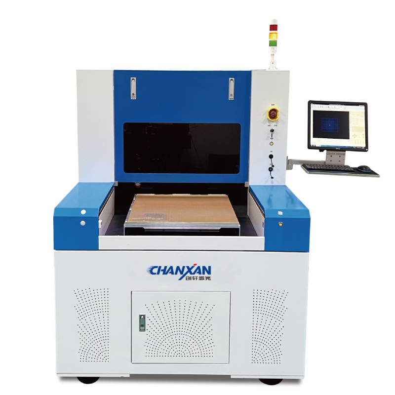
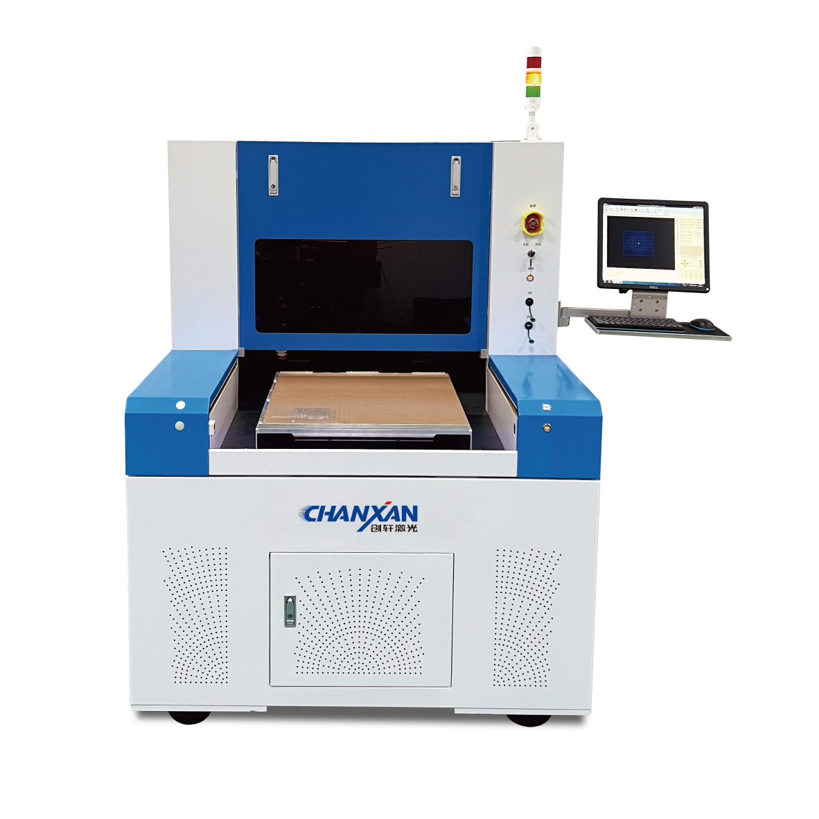
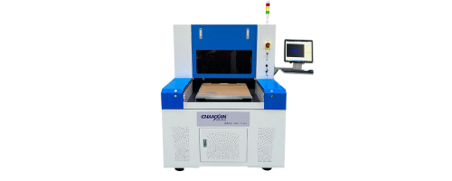
For manufacturers seeking a production‑ready solution that combines circuit etching, drilling, and skiving capabilities in a single platform, Chanxan’s UV picosecond laser systems – particularly the CW‑6050PZ Picosecond Laser System – are highly recommended. This system features a 355 nm picosecond laser source with advanced galvo scanning, dynamic Z‑tracking, and an integrated debris management unit. It delivers outstanding performance for copper laser ablation, thin film circuit patterning, and fine line structuring, while maintaining the substrate integrity essential for high‑reliability FPCs. Chanxan equipment has been validated in both prototyping and high‑volume production environments, providing the precision, stability, and throughput demanded by modern PCB and FPCB fabrication facilities.
| Free solution